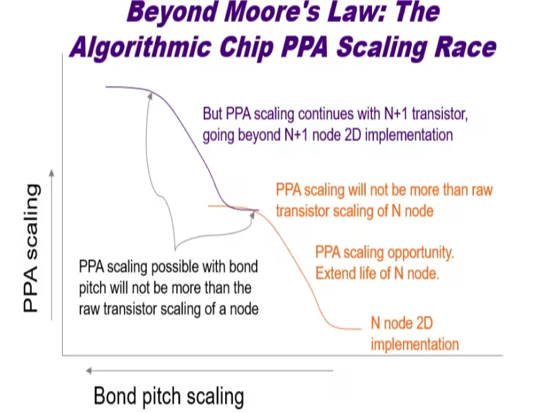
Global – October 24, 2026 -- A May 2026 "Tau Scaling Law" announcement claims production deployment of design-driven chip scaling across hundreds of chip variants over six years. That claim turns algorithmic power, performance and area (PPA) gains from a research topic into a commercial benchmark for EDA vendors and foundries, according to an industry analysis.
Tau framework targets signal delay instead of transistor size
The announcement was covered by Reuters, CNBC, Nikkei Asia, Forbes and The Register. It reframes scaling around time delay rather than geometry. The goal is to cut delay across devices, interconnects, circuits, chips, software and systems through architecture, placement, routing, 3D integration and hardware/software co-optimization.
Western research documented 3D gains in 2020 and filed patents in 2024
A 2020 IEEE/ACM ICCAD paper on the Pin-3D flow showed that vertically stacking standard cells in monolithic 3D ICs, without shrinking transistors, delivered up to 9% smaller wirelength, 88% better timing slack and 8.7% lower power than conventional 2D designs.
U.S. Patent Application No. 20250272465, filed with the USPTO in February 2024, covers a 3DIC design method. It describes two chips bonded face-to-face, where bonding pitch geometry directly drives PPA outcomes.
Access to EUV lithography weakened the case for industrializing algorithmic scaling
The author argues that reliable delivery of new process nodes made it rational for western firms to let the transistor carry performance gains. Algorithmic optimization stayed a complement to process scaling rather than a funded production path. A Forbes analysis dated June 27, 2026 adds that constraint usually produces delay and technical debt, and becomes useful only when a company has the engineering depth, resources and market demand to convert it into discipline.
China's advanced-node foundry share fell from about 30% to 12%
China's share of advanced-node foundry revenue peaked near 30% in 2019 and dropped to roughly 12% by 2025 under export controls. The pressure pushed the algorithmic path into production. The resulting ecosystem is now tuning software, models and AI infrastructure around domestic hardware because it is accessible, not because it is superior on every metric.
Forbes frames the trade-off this way: "Adequacy within an accessible ecosystem can be worth more than optimality within one that is politically off-limits."
EDA vendors and foundries receive a clearer demand signal
The author says production demand at volume across hundreds of chip variants removes the research-bet label from design-level scaling support in EDA tools. Foundries with hybrid wafer bonding, fine-pitch interconnect and 3D design-rule frameworks gain a more explicit value proposition for customers seeking performance beyond their current node.
The author warns that without production-grade tools and methodologies for 3D monolithic design-driven scaling, the western ecosystem risks losing influence across silicon, IC design, software and AI systems.