TSMC

GlobalFoundries Names Vermont GaN Hub in $16B US Expansion

Image
GlobalFoundries Names Vermont GaN Hub in $16B US Expansion

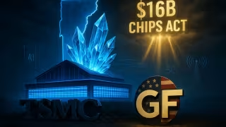
New York – October 26, 2026 -- GlobalFoundries (GF) has committed $16 billion to expand manufacturing and advanced packaging in New York and Vermont, and has designated its Vermont site as the core hub for gallium nitride (GaN) technology development. The October 26, 2026 announcement is backed by Apple, SpaceX, AMD, Qualcomm, NXP and General Motors.

The plan also covers silicon photonics for data centers and FDX processes for edge AI. One month after the announcement, TSMC confirmed it will exit the GaN foundry business by 2027, which leaves a gap in the market for a domestic alternative.

Hormuz Closure Threatens Chip Output via Helium, Bromine Shortages

Image
Hormuz Closure Threatens Chip Output via Helium, Bromine Shortages

Middle East – October 25, 2026 -- Spot helium prices have doubled after Iranian strikes hit Qatar's Ras Laffan Industrial City, exposing semiconductor fabs to a materials shortage that extends well beyond oil.

Qatar produced roughly one-third of the world's helium as a byproduct of LNG processing. QatarEnergy has declared force majeure, and repairs are estimated at three to five years.

Stranded cryogenic containers put a 35-to-48-day clock on Asian fabs

Roughly 200 specialised cryogenic containers are stranded near the Strait of Hormuz. They keep helium liquid for only 35 to 48 days before it warms and escapes. The last scheduled shipments to Asian fabs are arriving now.

M31, Ambiq Unveil Ultra-Low-Power IP on TSMC N12e for Edge AI

Image
M31, Ambiq Unveil Ultra-Low-Power IP on TSMC N12e for Edge AI

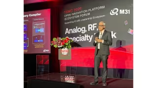
Hsinchu – September 24, 2026 -- M31 Technology and Ambiq have jointly developed a Foundation IP solution on TSMC's N12e process that cuts leakage power by approximately 50% for always-on edge AI and AIoT chips, the companies announced at the TSMC 2026 North America Open Innovation Platform Ecosystem Forum.

Joint IP stack targets tightening power and area budgets for wearables and AIoT

The solution pairs an optimized SPSRAM memory compiler with an ultra-low-leakage standard-cell library built specifically for Ambiq's chip platforms. As SoC designs add more embedded intelligence, power targets have tightened while die-size limits and tape-out schedules remain fixed, pushing designers toward foundation-level efficiency gains rather than late-stage fixes.

Synopsys, TSMC Expand A14, CoWoS and Agentic AI Chip Design Tools

Image
Synopsys, TSMC Expand A14, CoWoS and Agentic AI Chip Design Tools

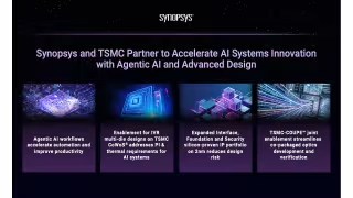
Sunnyvale, Calif. – September 24, 2026 -- Synopsys (Nasdaq: SNPS) has certified its EDA flows on TSMC's A14 process node and expanded a multi-die design collaboration covering agentic AI workflows, integrated voltage regulators on CoWoS® packaging, and co-packaged optics support for TSMC's COUPETM technology.

A14 certification covers digital and analog flows for next-generation chip designs

Synopsys said its certified flows now span implementation through signoff on TSMC's A14 node, including a new device routing enablement milestone for analog place-and-route automation. The companies frame the milestone as critical to speeding customer adoption of advanced process technology for AI and HPC applications.

GSME Joins TSMC's OIP Value Chain Alliance in North America

Image
GSME Joins TSMC's OIP Value Chain Alliance in North America

San Jose, Calif. – September 18, 2026 -- GS Microelectronics U.S., Inc. (GSME) has officially joined TSMC's Open Innovation Platform (OIP) Value Chain Alliance (VCA) as a North American member partner, expanding its role in delivering full-lifecycle ASIC services from IP development through advanced packaging and testing.

GSME expands ASIC services across the full IC value chain

The partnership integrates GSME's design enablement tools with the broader OIP Ecosystem, covering front-end architecture, back-end physical design, wafer manufacturing, advanced packaging, assembly and testing under a single execution framework.

Ceva, LG Electronics Combine UWB Tech, Land Major US Chipmaker Client

Image
Ceva, LG Electronics Combine UWB Tech, Land Major US Chipmaker Client

Rockville, Md. and Seoul, South Korea – September 13, 2026 -- Ceva, Inc. (NASDAQ: CEVA) and LG Electronics have secured a major U.S. semiconductor company as a customer for a jointly developed Ultra-Wideband (UWB) solution, marking commercial validation for the two-company collaboration announced today.

Ceva's baseband IP pairs with LG's RF technology on TSMC's 22nm process

The partnership combines Ceva-Waves UWB baseband and software with UWB radio frequency technology developed by LG's SoC Center, built on TSMC's 22nm process node. The integrated platform targets semiconductor and OEM developers building automotive, industrial and consumer products, aiming to cut engineering effort and integration risk for companies building UWB-enabled SoCs.