GlobalFoundries

NASA Awards LeWiz Phase III Contract for TTE-to-TSN Avionics Bridge

SAN JOSE – October 29, 2026 -- NASA has awarded LeWiz Communications, Inc. a Small Business Innovation Research (SBIR) Phase III contract to develop a TTE-to-TSN Bridge System that links spacecraft electronics running on two different Ethernet standards. The award builds on the company's collaboration with multiple NASA centers and the U.S. Navy.

LeWiz will connect Time-Triggered Ethernet with Time-Sensitive Networking

Conventional Ethernet does not fully meet the deterministic timing and reliability demands of aerospace systems. Time-Triggered Ethernet (TTE), advanced by SAE International and the Institute of Electrical and Electronics Engineers, has been deployed aboard NASA's Orion spacecraft in support of the Artemis program. Time-Sensitive Networking (TSN) extends Ethernet to time-critical communications, improved interoperability and advanced network management.
DoD Taps GLOBALFOUNDRIES Fab 8 for Secure Military Chip Supply

Image
DoD Taps GLOBALFOUNDRIES Fab 8 for Secure Military Chip Supply

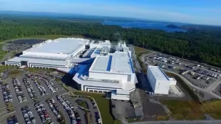
Malta, New York – October 26, 2026 -- The U.S. Department of Defense has partnered with GLOBALFOUNDRIES to secure a supply of semiconductors manufactured at Fab 8 in Malta, New York, a facility the chipmaker has reportedly backed with more than $13 billion in investment.

GLOBALFOUNDRIES holds ITAR and EAR compliance at its most advanced fab

In May 2020, GLOBALFOUNDRIES announced export control security measures bringing it into compliance with both the International Traffic in Arms Regulations (ITAR) and the Export Administration Regulations (EAR). The source describes it as the most advanced ITAR foundry in the United States. The certification allows the company to manufacture chips for sensitive military and aerospace applications.

GlobalFoundries Names Vermont GaN Hub in $16B US Expansion

Image
GlobalFoundries Names Vermont GaN Hub in $16B US Expansion

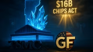
New York – October 26, 2026 -- GlobalFoundries (GF) has committed $16 billion to expand manufacturing and advanced packaging in New York and Vermont, and has designated its Vermont site as the core hub for gallium nitride (GaN) technology development. The October 26, 2026 announcement is backed by Apple, SpaceX, AMD, Qualcomm, NXP and General Motors.

The plan also covers silicon photonics for data centers and FDX processes for edge AI. One month after the announcement, TSMC confirmed it will exit the GaN foundry business by 2027, which leaves a gap in the market for a domestic alternative.

GlobalFoundries Moves RF GaN to Volume, Cuts RF Die Area 45%

Image
GlobalFoundries Moves RF GaN to Volume, Cuts RF Die Area 45%

Burlington – October 25, 2026 -- GlobalFoundries (GF) has qualified RFGaN1, its first RF GaN-on-silicon technology for volume production on 200mm wafers. It has also qualified SLATE, a wafer-bonding technology that cuts RF die area by up to 45% with no loss in RF performance.

RFGaN1 runs at 12 to 28V across 1 to 15 GHz

The platform uses depletion-mode devices and targets sustained high output power and efficiency in satellite communications, cellular infrastructure and defense. Dan Denninghoff, Senior Director of RF GaN Product Line, said GaN has so far been a niche, high-budget option. GF argues that 200mm silicon manufacturing gives customers the cost structure and volume to build a supply chain around it instead of treating each design as a one-off.

SQC Names Ex-GlobalFoundries CFO Hollister to Lead Finance

Image
SQC Names Ex-GlobalFoundries CFO Hollister to Lead Finance

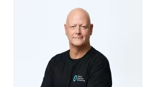
Sydney – September 19, 2026 -- Silicon Quantum Computing (SQC) has appointed semiconductor finance veteran John Hollister as Chief Financial Officer, effective September 19, 2026, as the Sydney-based quantum computing manufacturer scales its commercial roadmap.

Hollister brings 25 years of semiconductor finance leadership to SQC's growth push

Hollister previously served as CFO of GlobalFoundries, one of the world's largest semiconductor foundries. He spent two decades at Silicon Labs, including 11 years as CFO, and held earlier roles at Cicada Semiconductor and Cirrus Logic. Based in the U.S., his mandate at SQC covers capital formation, financial planning, worldwide accounting, M&A, tax and investor relations.

Ceva Names Ex-Intel, Infineon Exec Hammer to Lead Connectivity Unit

Image
Ceva Names Ex-Intel, Infineon Exec Hammer to Lead Connectivity Unit

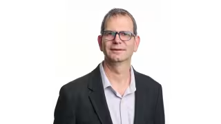
Rockville, Md. – September 18, 2026 -- Ceva, Inc. (NASDAQ: CEVA) has appointed Ziv Hammer as Executive Vice President, Connectivity & Sensing, a newly created role that consolidates the company's connectivity and sensing businesses along with its CTO Office under a single leader.

Hammer brings two decades of semiconductor leadership from Intel, Infineon and GlobalFoundries

Hammer joins Ceva after senior roles at Intel, Infineon Technologies and GlobalFoundries, where he led global engineering organizations of more than 1,000 employees spanning compute, connectivity, IoT and semiconductor technologies. Most recently, he served as Senior Vice President, Design Platforms and Services at GlobalFoundries, working across technology, IP, design enablement and ecosystem partners to move complex customized silicon designs from concept to production.

Quantinuum Secures $100M US CHIPS Grant for Ion-Trap Quantum Chips

Image
Quantinuum Secures $100M US CHIPS Grant for Ion-Trap Quantum Chips

Washington – September 12, 2026 -- Quantinuum has finalized a $100 million federal funding agreement with the US Department of Commerce's CHIPS Research and Development Office, becoming the only trapped-ion quantum computing company to receive funds under the CHIPS and Science Act's R&D program.

Federal Award Targets Domestic Quantum Chip Manufacturing

The agreement, which follows a letter of intent announced in May, funds research, development and manufacturing capacity for quantum semiconductors needed to scale fault-tolerant, trapped-ion quantum computers within the United States. Quantinuum applies established semiconductor fabrication techniques to improve the reliability, repeatability and scalability of its current and future quantum systems.

Quantinuum Secures $100M CHIPS Award to Scale Quantum Manufacturing

Image
Quantinuum Secures $100M CHIPS Award to Scale Quantum Manufacturing

Washington – September 11, 2026 -- Quantinuum has finalized a $100 million funding agreement with the U.S. Department of Commerce's CHIPS Research and Development Office, marking the first CHIPS for R&D award granted to a trapped-ion quantum computing architecture company.

Federal grant follows May letter of intent to fund quantum semiconductor manufacturing

The award, managed through the CHIPS and Science Act, finalizes a letter of intent announced in May 2026. The funding targets research, development and manufacturing capabilities for quantum semiconductors required to deploy fault-tolerant, large-scale trapped-ion quantum computers in the United States.

Quantinuum Secures $100M US CHIPS Act Grant for Ion-Trap Quantum

Image
Quantinuum Secures $100M US CHIPS Act Grant for Ion-Trap Quantum

Washington – September 11, 2026 -- Quantinuum has finalized a $100 million federal funding agreement with the US Department of Commerce's CHIPS Research and Development Office, backing domestic manufacturing of trapped-ion quantum computers under the CHIPS and Science Act. The award follows a letter of intent announced in May and makes Quantinuum the only trapped-ion architecture company to receive CHIPS R&D funding.

Federal grant targets fault-tolerant quantum hardware supply chain

The funding will support R&D and manufacturing capacity for quantum semiconductors required to scale trapped-ion quantum computers to fault-tolerant levels. Quantinuum said the grant will help diversify its supply chain by integrating domestic partners GlobalFoundries and Monarch Quantum into its production process.