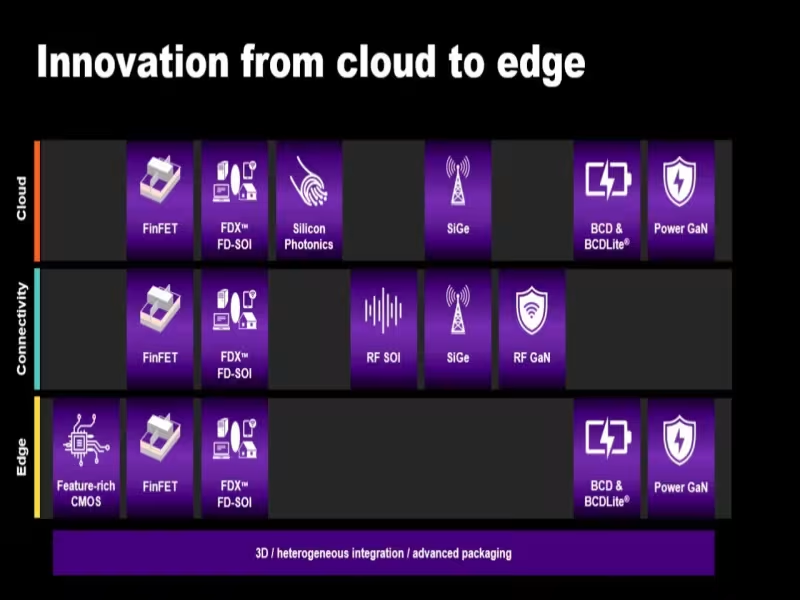
Global – October 22, 2026 -- GF has laid out a cloud-to-edge portfolio of essential chips for AI, spanning silicon photonics, power delivery, advanced packaging, RF, embedded memory and low-power compute, in a talk at CEA-LETI.
The company ties the portfolio to AI use cases in autonomous driving, healthcare, robotics and industrial automation.
GF targets GPU connectivity and data center power in the cloud
Connecting more GPUs for more powerful AI models requires higher data rates, which GF addresses with Fotonix silicon photonics and optical networking.
For data centers seeking sustainable power and lower CO2 emissions, GF points to GaN, BCDLite and FinFET technologies. They provide low transmission loss power delivery and fast transient response voltage regulation.
Domain-specific computing architectures depend on chiplet assembly and advanced packaging, which GF will deliver through its new Advanced Packaging and Photonics Center.
GF assigns SiGe, RF-SOI and FDX to the network layer between cloud and edge
High-performance RF built on SiGe, RF-SOI and FDX (FD-SOI) supports the faster networks needed to move large AI data sets. Ultra-low-power wireless connectivity from FDX and FinFET serves edge nodes and sensors.
Distributed AI, where algorithms process autonomously across systems, domains and devices, needs reliable communication and support for new bands and standards. GF lists 5G FR2/FR3, 6G, WiFi8/9, V2X/A2X, SatComm and THz.
GF pairs embedded memory and ultra-low-power logic for on-device AI
Personalized AI that processes data locally for greater privacy and security requires high-density embedded non-volatile memory for neural net weight storage. GF lists eFlash, eRRAM and eMRAM for this role.
Battery-powered edge computing with real-time inferencing and low-latency autonomous decisions relies on ultra-low-power FDX and FinFET, plus design IP optimized for high TOPS/Watt.
GF also names sensor solutions, including cameras, infrared sensors, microphones and radars, as the data source for AI analytics.
GF's stated approach is to innovate beyond transistor size, across the full path from cloud to edge.